- 您现在的位置:买卖IC网 > Sheet目录312 > AT26DF081A-SSU (Atmel)IC FLASH 8MBIT 70MHZ 8SOIC
�� �
�
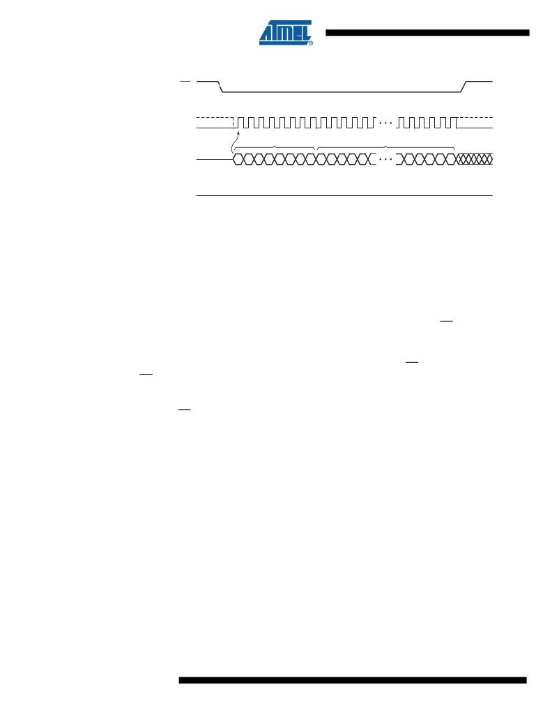
�Figure� 8-5.�
�C� S�
�Block� Erase�
�0�
�1�
�2�
�3�
�4�
�5�
�6�
�7�
�8�
�9�
�10� 11� 12�
�26� 27� 2� 8� 2� 9� 3� 0� 3� 1�
�S� CK�
�OPCODE�
�ADDRE� SS� BIT� S� A2� 3� -A0�
�S� I�
�C�
�C�
�C�
�C�
�C�
�C�
�C�
�C�
�A�
�A�
�A�
�A�
�A�
�A�
�A�
�A�
�A�
�A�
�A�
�A�
�M� S� B�
�M� S� B�
�S� O�
�HIGH-IMPEDANCE�
�8.4�
�Chip� Erase�
�The� entire� memory� array� can� be� erased� in� a� single� operation� by� using� the� Chip� Erase� command.�
�Before� a� Chip� Erase� command� can� be� started,� the� Write� Enable� command� must� have� been� pre-�
�viously� issued� to� the� device� to� set� the� WEL� bit� of� the� Status� Register� to� a� logical� “1”� state.�
�Two� opcodes,� 60h� and� C7h,� can� be� used� for� the� Chip� Erase� command.� There� is� no� difference� in�
�device� functionality� when� utilizing� the� two� opcodes,� so� they� can� be� used� interchangeably.� To�
�perform� a� Chip� Erase,� one� of� the� two� opcodes� (60h� or� C7h)� must� be� clocked� into� the� device.�
�Since� the� entire� memory� array� is� to� be� erased,� no� address� bytes� need� to� be� clocked� into� the�
�device,� and� any� data� clocked� in� after� the� opcode� will� be� ignored.� When� the� CS� pin� is� deasserted,�
�the� device� will� erase� the� entire� memory� array.� The� erasing� of� the� device� is� internally� self-timed�
�and� should� take� place� in� a� time� of� t� CHPE� .�
�The� complete� opcode� must� be� clocked� into� the� device� before� the� CS� pin� is� deasserted,� and� the�
�CS� pin� must� be� deasserted� on� an� even� byte� boundary� (multiples� of� eight� bits);� otherwise,� no�
�erase� will� be� performed.� In� addition,� if� any� sector� of� the� memory� array� is� in� the� protected� state,�
�then� the� Chip� Erase� command� will� not� be� executed,� and� the� device� will� return� to� the� idle� state�
�once� the� CS� pin� has� been� deasserted.� The� WEL� bit� in� the� Status� Register� will� be� reset� back� to�
�the� logical� “0”� state� if� a� sector� is� in� the� protected� state.�
�While� the� device� is� executing� a� successful� erase� cycle,� the� Status� Register� can� be� read� and� will�
�indicate� that� the� device� is� busy.� For� faster� throughput,� it� is� recommended� that� the� Status� Regis-�
�ter� be� polled� rather� than� waiting� the� t� CHPE� time� to� determine� if� the� device� has� finished� erasing.� At�
�some� point� before� the� erase� cycle� completes,� the� WEL� bit� in� the� Status� Register� will� be� reset�
�back� to� the� logical� “0”� state.�
�The� device� also� incorporates� an� intelligent� erasing� algorithm� that� can� detect� when� a� byte� loca-�
�tion� fails� to� erase� properly.� If� an� erase� error� occurs,� it� will� be� indicated� by� the� EPE� bit� in� the�
�Status� Register.�
�14�
�AT26DF081A�
�3600G–DFLASH–06/09�
�发布紧急采购,3分钟左右您将得到回复。
相关PDF资料
AT26DF161-SU
IC FLASH 16MBIT 66MHZ 8SOIC
AT26DF161A-MU
IC FLASH 16MBIT 70MHZ 8QFN
AT26DF321-SU
IC FLASH 32MBIT 66MHZ 8SOIC
AT27BV010-90JU
IC OTP 1MBIT 90NS 32PLCC
AT27BV020-90JU
IC OTP 2MBIT 90NS 32PLCC
AT27BV040-12JU
IC OTP 4MBIT 120NS 32PLCC
AT27BV1024-90JU
IC OTP 1MBIT 90NS 44PLCC
AT27BV256-70JU
IC OTP 256KBIT 70NS 32PLCC
相关代理商/技术参数
AT26DF081A-SSU-RET
制造商:Atmel Corporation 功能描述:
AT26DF081A-ST-B
制造商:Adesto Technologies Corporation 功能描述:8-SOIC-W, AUTO GRADE 3, 2.7V, TUBE - Rail/Tube
AT26DF081A-ST-T
制造商:Adesto Technologies Corporation 功能描述:8-SOIC-W, AUTO GRADE 3, 2.7V, T&R - Tape and Reel
AT26DF081A-SU
功能描述:闪存 8M 8 I/O Pins SPI 256B 2.7V-3.6V RoHS:否 制造商:ON Semiconductor 数据总线宽度:1 bit 存储类型:Flash 存储容量:2 MB 结构:256 K x 8 定时类型: 接口类型:SPI 访问时间: 电源电压-最大:3.6 V 电源电压-最小:2.3 V 最大工作电流:15 mA 工作温度:- 40 C to + 85 C 安装风格:SMD/SMT 封装 / 箱体: 封装:Reel
AT26DF081-MU
制造商:Adesto Technologies Corporation 功能描述:SF DATAFLASH, 8M, MLF, IND TEMP,GREEN - Trays
AT26DF081-SU
制造商:Adesto Technologies Corporation 功能描述:SF DATAFLASH, 8M, SOIC ,IND TEMP, GREEN - Rail/Tube
AT26DF161
制造商:ATMEL 制造商全称:ATMEL Corporation 功能描述:16-megabit 2.7-volt Only Serial Firmware DataFlash Memory
AT26DF161_06
制造商:ATMEL 制造商全称:ATMEL Corporation 功能描述:16-megabit 2.7-volt Only Serial Firmware DataFlash Memory